

Introduction
Materials found in nature often aren’t directly utilised in their existing forms for engineering purposes. Instead, scientists find ways to modify them to make the best use of their unique properties. For instance, in communication technology, the size, shape and orientation of materials is altered to change their interaction with electromagnetic waves of different wavelengths. Today, it is possible to change the properties of light using nano-sized metasurfaces instead of optical lenses. Metasurfaces are actually thin layers of two-dimensional metamaterials (artificially crafted materials) that allow or inhibit the propagation of electromagnetic waves in desired directions. Optical metasurfaces can locally impart changes to phase, amplitude, and polarization of propagating waves. A significant advancement in nanophotonics was achieved by researchers at IIT Bombay as they developed a novel AI based numerical method to study the interaction of metasurfaces with light.
How did the research come about?
This interdisciplinary research was a result of a collaboration between researchers of Physics department Mr. Abhishek Mall & Prof. Anshuman Kumar and Electrical department Mr. Abhijeet Patil & Prof. Amit Sethi at the Indian Institute of Technology Bombay, Mumbai, India. Mr. Mall initially came up with an idea for this research and discussed its implementation with his colleges. He generated the training dataset and then all of them participated in the data analysis, writing, and reading of the research paper. Prof. Sethi and Prof. Kumar managed the project and finally their study was published in the journal Scientific Reports by Springer Nature. The project was funded by the Department of Science and Technology, Government of India, and the Industrial Research and Consultancy Centre, IIT Bombay. The researchers were interviewed and an article highlighting their research was written by Mr. Debdutta Paul and published under R&D dissemination initiative of IRCC.
Background work
The team of researchers created a metasurface consisting of a layer of silicon sandwiched between two layers of gold. Four different designs were created by
modifying the geometric shapes of the topmost gold layer, which is a few
nanometres thick. Researchers noticed that as metamaterials interact with the
incoming beam of light, it gets amplified. In practical purposes, “the amplification makes it much easier to detect small changes in the light shone on the surface,” says Mr. Mall. It was of interest to study how the metasurfaces affect the ‘polarization’ of light. The researchers used a computer to virtually shine a light with certain polarization and aimed to generate light with the opposite polarization. To serve this purpose, ideally, “one needs to solve the Maxwell’s equations for input to each metasurface until we get the desired output,” Mr. Mall continued. However, solving them consumes a lot of time as well as computing power. “Moreover, the design process is limited by human intuition, and it is incredibly hard to develop the intuition in accurately solving the equations,” says Prof Kumar.
Developing the AI algorithms
In order to overcome the issues associated with the existing process, the team
decided to create a method to study the interaction between the light and the
metasurfaces without the need to solve complex Maxwell’s equations. The first step for the team was to develop an algorithm that predicts the geometrical design of the topmost gold layer in the metasurface necessary to generate the projected output beam. The algorithm is designed such that it produces geometrical designs based on optical response and gradually improves its design by comparing it with the actual design. For the algorithm to work well, it needed to predict results as we get after solving the Maxwell’s equations. So, the team solved the Maxwell’s equations for the required geometries and successfully verified that algorithm appropriately predicted the optical response. But, every time verifying the results from the algorithm by solving Maxwell’s equations was not a good idea. In order to avoid this, the team created another algorithm to mimic the solution of Maxwell’s equations itself. They just needed to feed the geometry of the nano-sized gold layer to the algorithm to get the corresponding optical response.
“This technique is a form of Artificial Intelligence. Such AI based technologies are everywhere today from our shopping lists, video recommendations, online advertising, assisted medical diagnosis, self-driving cars, and search engines,” says Prof Kumar revealing that these algorithms are based on AI while acknowledging the critical role AI is playing in modern society.
The above two algorithms were combined to carry out the entire process of identifying the correct geometrical pattern for the required response and validating it against the Maxwell’s equations. Unbelievingly, this complete process takes only about 11 milliseconds to predict the correct geometric configuration! One more advantage of this algorithm is that the user can define any thickness as needed. “Currently, we are implementing our algorithm to work with more stringent requirements that the user would like to specify. We also want these metasurfaces to be very light and thin, to achieve the best of both worlds,” Prof. Kumar signs off.
Understanding in-depth
The conventional approach for designing and optimizing the nanophotonic
metasurface as per the target electromagnetic response involves exploring large geometry and material spaces. This is a highly iterative process based on trial and error which is computationally costly and time consuming. This problem is also challenging because the structural designs aren’t unique and their relationship with the corresponding electromagnetic responses is non-linear. The researchers have modelled this ‘unintuitive’ relationship as a probability distribution in the design space by introducing a framework based on cyclical deep learning (DL).
Now DL is a data-driven method. It can learn highly non-linear functions mapping the inputs to the outputs in a training dataset by using deep artificial neural networks (NNs) with layer architectures which allow training using convex optimization technique despite their depth. With a sufficient amount of training data and regularization techniques, the learned representation from DL can generalize to unseen datasets. However, earlier methods using fully connected (FC) NNs and convolutional neural networks (CNNs) either encounter the limitation of optimizing a single candidate design or the requirement of a large dataset for training. Other NN architectures address the inverse design of nanophotonic metasurface as a regression problem, mapping optical response to structural design space. This approach though, forces the network to converge to one of the several solutions and so, no new designs are generated. Thus, more flexible DL methods were desired.
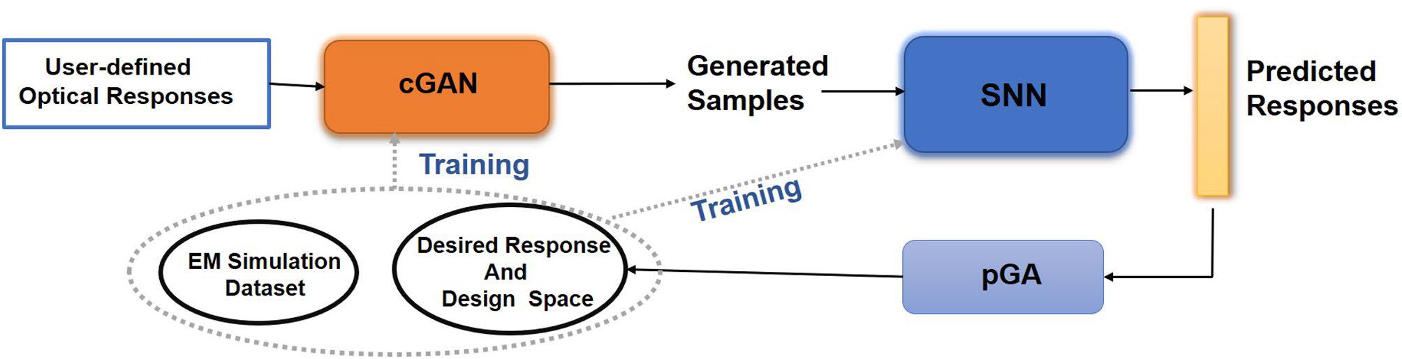
The team proposed cyclical generation and discovery of metasurfaces for user-defined optical response, with no structural design restrictions. Their framework includes consecutive DL models that emulate both numerical electromagnetic simulation and iterative processes of optimization to generate optimized structural designs while simultaneously performing forward and inverse design tasks.
For the training and evaluation, the researchers generated a dataset of 1500
Aluminum (Al)-nanoantennae samples with four classes of structural design of
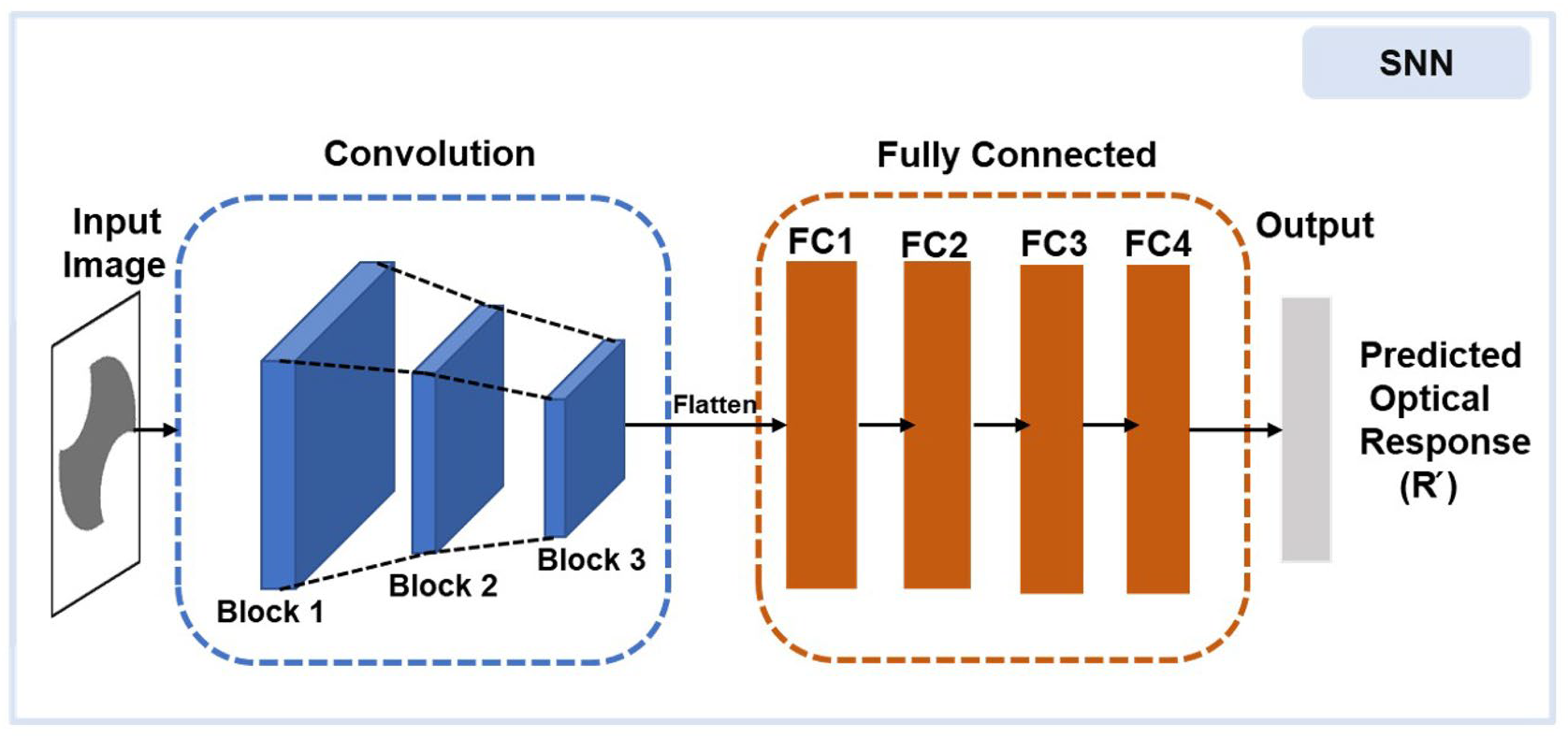
different dimensions. To predict the optical response (forward design) they used Simulation Neural Network (SNN) because an efficiently trained SNN acts as an efficient numerical electromagnetic simulation solver that can predict an optical response in a few milliseconds on even a general purpose laptop. It takes 2D cross-sectional structural design image as input and predicts its optical response.
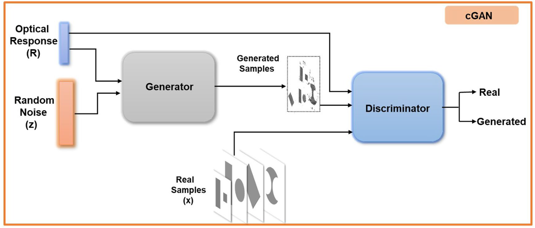
A conditional generative adversarial network (cGAN) is used to model the
probabilistic distribution of the design space (inverse design). This is because, upon training, it not only generates new structural designs but also ensures that these have optical response with features similar to the EM simulated dataset samples. The cGAN model architecture consists of two networks: a generator (G) and a discriminator (D). G accepts optical response and a random noise distribution z to generate structural design. D evaluates real structural designs from generated structural designs as real or fake. G consists of five transposed convolutional layers, while D consists of five convolutional and two FC layers.
The pseudo genetic algorithm (pGA) is applied to the optical responses to sort designs by minimal variation between their predicted and desired optical responses through selection and evaluation process. This along with the models together forms a pseudo generation framework: It takes as input a batch of user-defined optical responses and generates good-quality structural designs with authentic optical response using cGAN and SNN respectively, and is characterized into desired response and design space via pGA. In each cycle, the EM simulation and new generated data samples are used as an updated dataset for training.
For the evaluation of trained DL models, they measured the accuracy of the
predicted optical response by SNN and authenticity of optical response of generated designs through cGAN, using two metrics: MSE and cosine similarity. They found that their optimized framework generates structural designs with 0.021 mean square error and 0.968 cosine similarity, while also discovering new metasurface designs. Indeed, the prediction of optical responses using SNN took only a few milliseconds per sample. The results demonstrate that the design of metasurfaces by this technique is rapid and accurate. Their framework is a powerful tool to reduce the cost of computation and optimize nanophotonic design efficiency while exploring new designs. This can have significant importance in speeding up several technological applications in optics.
Sources:
IITB Research Highlight Article - Novel AI-based algorithms on well-known physics can speed up technology
Research Paper - Mall, A., Patil, A., Sethi, A. et al. A cyclical deep learning based framework for simultaneous inverse and forward design of nanophotonic metasurfaces. Sci Rep 10, 19427 (2020)