We can’t imagine our lives without these awesome techs we posses in our hands right now, especially in the global pandemic. From online lectures/meetings & webinars to the OTT platforms & high-definition games we enjoy is all because of those silicon chips that resides underneath every gadget we use or see. Within past 30 years engineers & scientists worked continuously to make these silicon chips smaller & smaller to the extent of the size of our fingernails & having billions of these tiny silicon transistors (an electrical switch) within it!

But now we have reached to a limit. As the size is reducing to an extent of 3 to 7 nanometers technology (i.e. size of those silicon transistors in the silicon chip), we are now facing issues of overheating, data rot, slower speed, etc. This is because the current technology is primarily based on charge of an electrons as a binary state. Due to tremendous reducing the size, we not only face the problem of overheating, but most importantly the problem of data rot of the files we store in our SD cards, portable SSD’s, pen drives, etc., mainly due to slightly imperfections in the insulation in the microscopic level.
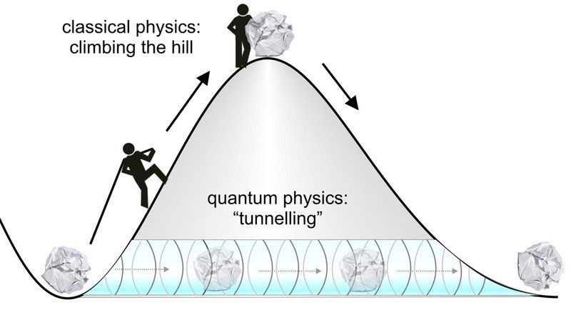
Another reason behind this data degradation & failed execution of a program/software is due to a very fascinating phenomena that comes under quantum mechanics known as quantum tunneling. As the thickness of the insulation is of the order of ~10 atoms, electron can just pass through the barrier irrespective of the equivalent potential barrier energy it needs to overcome the insulation.

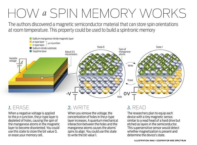
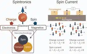
To overcome this challenge, rather than using the charge of an electron as our binary state, spin of an electron can used for the same. As every elementary particle (here an electron) either possess spin up or spin down, these can be assigned as a binary logic 1/0. The branch which especially works/studies on this intrinsic property of electron on electronics is known as spin transport electronics or commonly called as spintronics.
There are many advantages of a spintronic based device over an electronic device. A few of them are: -
1. They consume less power than that traditional silicon chips & thus less heat dissipation, therefore more battery life
2. As spin of an electron can be easily manipulated, thus the read-write speed will be extremely fast, making the devices like smart phones or computers work like a charm
3. Takes lesser space on chip, thus making the device thinner, sleek & compact
4. Doesn’t require any specially doped semiconductors, as iron, aluminium or silver will be required, making the cost of these devices lesser in comparison
5. And the most important advantage of all no memory leak, or data rot concept will exist, thus our files, pictures, videos, etc will no longer get corrupted over a longer period of time (maybe over generations).
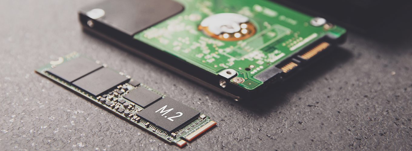
Now there are devices that are currently based on spintronics & we might be using one of them right now, the HHD’s or hard drives, since they use magnetic domains in the special platter/disk inside as there magnetic bits (1’s/0’s). Due to the moving parts inside HHD’s, it makes the device to be handled carefully, low read-write speed in comparison to those SSD’s, vulnerable to strong magnetic fields applied externally & mechanical wear & tear & only serve as a memory based device not a logical based device (like a microprocessor).
Assistant professor Dr.Chandrasekhar Murapaka of Indian Institute of Technology Hyderabad & assistant professor Dr.Arabinda Haldar of Indian Institute of Technology Hyderabad with their PhD students, collaborated with National Institute of Materials Science Japan & National Institute of Science Education and Research are trying to develop spintronic based memory & logic chips that can be even embedded on our powerful smartphones.
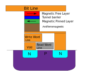
The idea behind this sci-fi tech in a nutshell is to have two ferromagnetic materials between them a thin insulator is sandwiched, making the system an electrical insulator. Now as those ferromagnetic materials will have all aligned spins of electrons respectively, keeping one of them have a fixed aligned spins of the electrons, making the fixed one to have spin up state (say) & by altering the total spins of electrons (all to be same at a time) in the later layer of ferromagnetic, the small electric current due to moving electrons can just tunnel (quantum tunnelling, as mentioned earlier) through our sandwich system depending on the relative spin state of the later ferromagnetic material to the fixed spin state of the initial ferromagnetic material. To get a proper clarity, SciToons (An educational YouTube channel) dedicated an entire video on the working of a spintronic device & their importance in practical world.

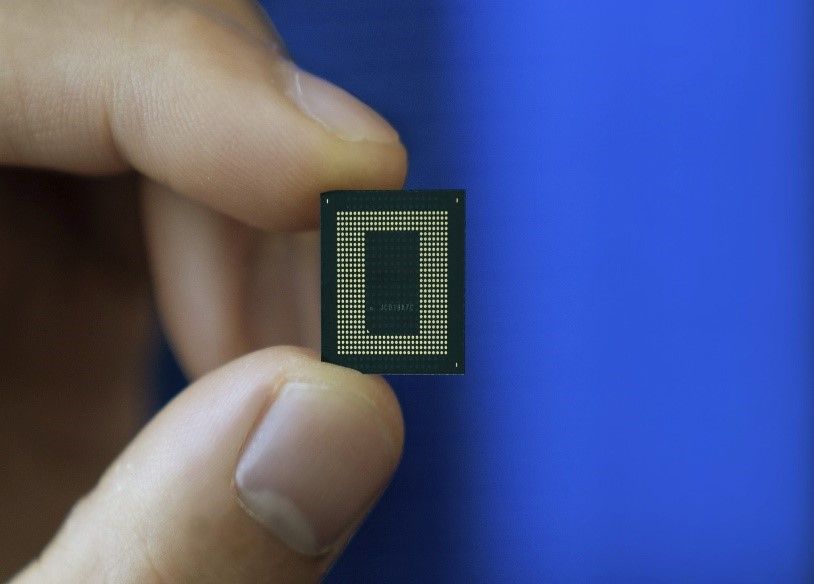
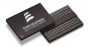
Now there are companies that commercialized the spintronic chips on industrial areas, research parks, etc. Companies like Everspin Technologies produces some spintronic memory chips on commercial scale, popularly known as MRAM’s.

The goal of this research team is to develop a logic based spintronic chip to achieve the goal of computational power like a microprocessor & to be economically viable for their mass production to devices like computers & smartphones. The success of this technology will not only change the entire experience to users like us but will certainly open the gates of inconceivable phenomena that are yet to be discovered especially in the domains of science & technology.